|
|
Your source of photonics CAD tools | |
|
| ||
FIMMPROPA bi-directional optical propagation tool |
   |
SOI 1x4 MMI Coupler Optimisation3D simulation and optimisation in silicon photonics with FIMMPROP and KallistosIn this example we combine FIMMPROP with our optimisation tool Kallistos to optimise a 1x4 MMI coupler in rigorous fully vectorial 3D for silicon photonics, based on an SOI buried waveguide geometry. Kallistos can take advantage of FIMMPROP's ability to scan design parameters very quickly, allowing us to investigate an extremely large number of structures in a small amount of time: on average we were able to investigate 8.3 designs per second! Although we focused on a silicon 1x4 MMI coupler, the same approach can be applied to any MMI design with any number of input and output branches.
Benefits of using FIMMPROP to model MMI couplersEME (EigenMode Expansion) is the ideal method to model MMI couplers. The physics of MMIs results from constructive and destructive interferences between a small number of guided modes; it is these interferences that give MMIs their ability to generate multiple images of the input beam. EME is a mode-based approach, and it therefore offers an extremely efficient way of modelling such devices. The implementation of EME in FIMMPROP offers an optimal framework for this application, with a potential for highly efficient optimisation and fully vectorial solutions:
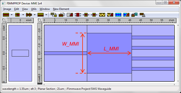
Design and parameterisation of the MMI designWe used a buried SOI waveguide geometry with a fixed silicon layer thickness of 220nm. We worked at a wavelength of 1.55um and used a refractive index of 3.5 for silicon and 1.44 for silica. We designed the MMI coupler using FIMMPROP's user interface. We used three variables to parameterise the structure: L_MMI and W_MMI to define the length and width of the central section, and a parameter alpha_out to control the gap between the output waveguides, expressed as a fraction of the width of the MMI.
You can see below how the parameter alpha_out works: if alpha_out is set to zero the gap is zero, if alpha_out is set to 1 the gap is maximised.
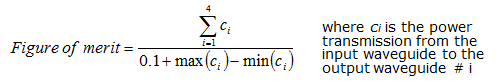
Figure of merit for the optimisationOur optimal design should provide us with low loss and a low imbalance between the power in the different output waveguides, so we asked Kallistos to look for designs that maximised the figure of merit shown below.
The optimiser was set up to vary the W_MMI and alpha_out. At each step of the optimisation, we got Kallistos to run a Python script which scanned the length of the MMI coupler and returned the optimal length for the selected values of W_MMI and alpha_out. Kallistos's ability to combine an optimiser with a script allowed us to run an optimisation with a very high level of complexity. As FIMMPROP can scan the length of a section instantly, this allowed us to obtain a much more efficient and finer optimisation than if we had included the length of the MMI in the optimisation settings. Preliminary studiesIdeal dimensions of input and output waveguidesWe used FIMMWAVE's Waveguide Scanner to study the effect of waveguide width on the effective index of the first order mode and found that the largest width to allow single-mode behaviour is 420nm. Such a small waveguide width leads to significant insertion losses, and we decided to use a larger width for the input and output waveguides. We will taper the waveguides to vary the waveguide width from the input and output waveguides to the single core waveguides used in the rest of the circuit. After a preliminary study we decided to set the width of the input and output waveguides to 1.5um, as this allowed us to keep insertion losses below 0.1dB. Minimum gap between output waveguidesWe then studied how large a gap we needed in between two output waveguides to minimise cross-coupling: we need to ensure that the cross-coupling is sufficiently low to permit the introduction of adiabatic tapers and the separation of the waveguides. Here again we used the Waveguide Scanner for a structure with two-branches and we studied the effect of the gap on the coupling length. We found that a gap of 0.15um between two branches gave a coupling length of 1mm, which we assumed would be sufficient. From this preliminary study we have established the following constraints on our design.
Performance of the optimiserOn a 8-core Xeon E5620 the optimiser calculated 29 iterations per hour; the modes were calculated semi-analytically with the FMM Solver. The SOI waveguide has a high index contrast and we generated mode profiles with a very high-resolution to calculate the overlaps with precision. At each iteration of the optimiser, Kallistos ran a script which controlled a FIMMPROP Scanner varying the length of the MMI coupler. The script ran a first scan of 512 different lengths with a step of 100nm and identified the optimum length; it then ran a second finer scan around the optimum to refine the results. Combine the optimiser with a script allowed
us to study over 712,700 structures in 24 hours: an average of 8.3
designs investigated per second, with a rigorous 3D fully vectorial
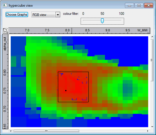
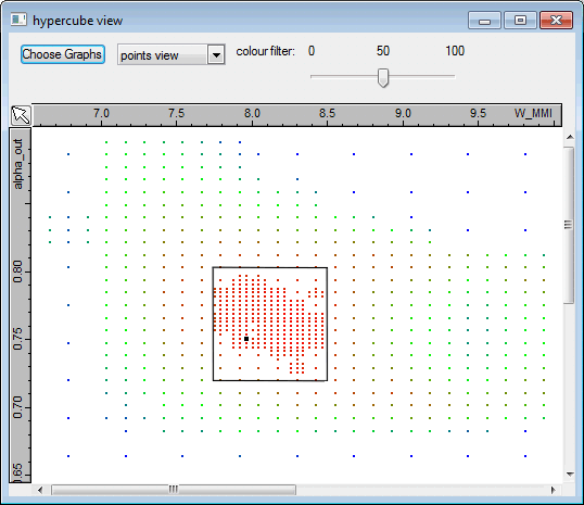
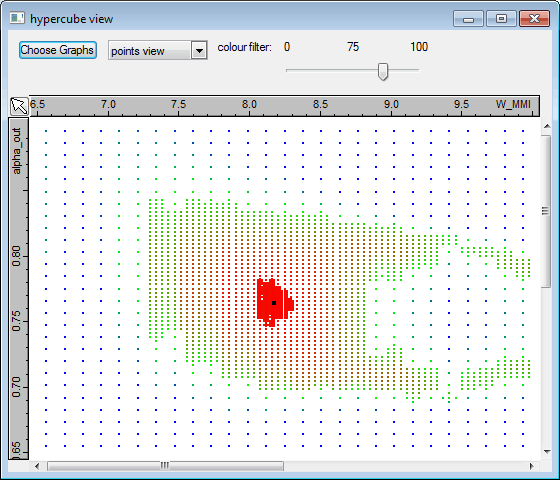
approach! Exploring the optimisation resultsKallistos allows you to visualise the optimisation data during the optimisation, and you can decide to pause and restart the optimiser in order to investigate the results and decide whether you want to push the optimisation further. You can see for instance what the optimisation data looked like after a first overnight run. The data is shown as calculation points on a map of the parameter space, with the width of the MMI W_MMI plotted in microns along the horizontal axis and the waveguide spacing parameter alpha_out plotted along the vertical axis. From this plot it is clear that we can narrow down the region of interest in the parameter space to the zone that we have delineated by a black line, in which the optimal results seem to be concentrated.
You can see here the same data, with each calculation point shown individually; as you can see the optimiser has already focused most of its efforts in the region that we have identified.
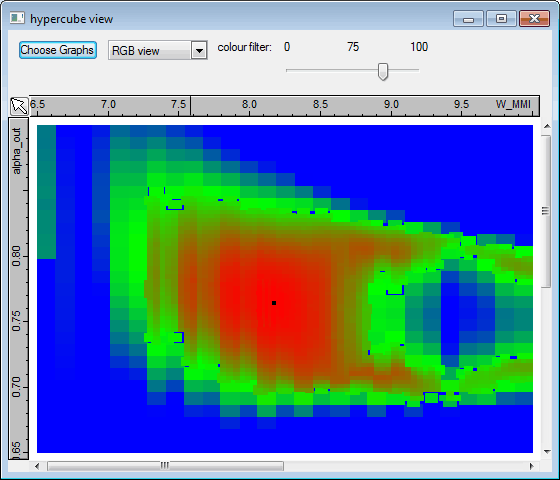
We decided to let the optimiser run for a little longer and this is the data that we eventually obtained.
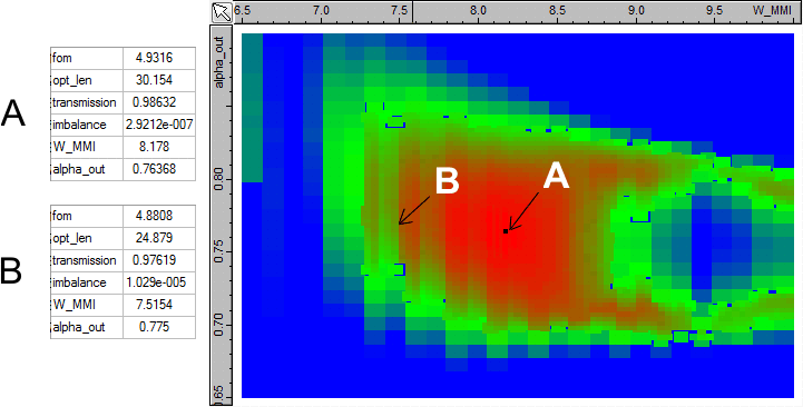
You can see in the graph below the position of the global optimum "A" in the optimisation space, at the centre of the optimum region. The properties and performance are shown on the left-hand side; "fom" is the figure of merit, "opt_len" is the optimal length of the MMI in microns, "transmission" is the sum of the power coupled to the four output waveguides and "imbalance" is the maximum discrepancy between the power in two output waveguides divided by the average output power. Design "A" corresponds to an optimum MMI length of 30.1um. As Kallistos allows us to visualise and post-process all the optimisation data we decided to look for the best design to allow us to keep the MMI length below 25um. The resulting design is shown below as design "B"; the imbalance is almost as good as design "A" but the total transmission dropped by 1%.
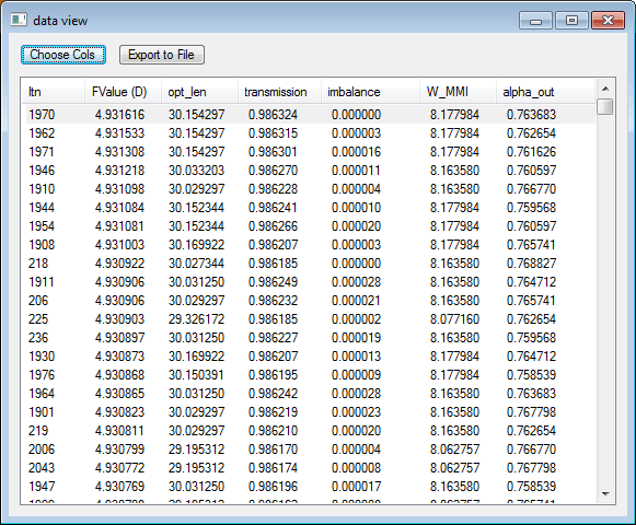
Kallistos is a fully transparent tool and you can inspect the data associated with each optimisation data point, allowing you to browse the raw data in order to find optima that correspond to your own criteria. For instance a global optimum might be located on the edge of a high-performance region, but you might choose as an optimal design a point located nearer the centre of the region in order to give you a better fabrication tolerance.
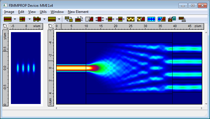
Performance of the optimal structuresWe used FIMMPROP to simulate the optimal designs that we identified from the Kallistos optimisation. You can see below the intensity profile for design A. The total loss is 0.060dB and the variation in power between the output waveguides is less than 0.00003% i.e. negligible.
|

 © 2023 Photon Design copyright all rights reserved |

 |