|
|
Your source of photonics CAD tools | |
|
| ||
OmniSimOmni-directional photonic simulations |
    |
Optical ring resonator filter model2D and 3D FDTD and FETD Simulations with OmniSim softwareFinite Difference Time Domain (FDTD) and Finite Element Time Domain (FETD) are ideal tools to model optical ring resonator filters and optical disk resonator filters of relatively small dimensions. OmniSim's user-friendly layout editor allows you to design optical ring resonators and optical disk resonators in just a few clicks, ready to simulate in 2D or 3D with our unique combination of FDTD and FETD algorithms. In 2D, our Finite Element Frequency Domain (FEFD) Engine will provide you with a highly reliable benchmark for your calculations.
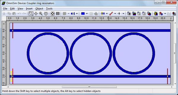
Note: for the modelling of large ring resonators (radii of 20um or more) or large ring resonator circuits, the computation time with an FDTD Engine can become very large even with a tool as fast as OmniSim. For the modelling of high Q resonators in 3D, you may need to run the FDTD calculation for a few days! Our propagation tool FIMMPROP combined with our photonic circuit simulator PICWave offers a very fast and rigorous alternative for the modelling of such structures. Design of a ring resonator in 2D using the OmniSim Layout EditorOmniSim's CAD interface allows you to design a ring resonator in just a few clicks by using pre-defined shapes. Shapes can be added and modified by simple drag and drop and you can adjust the parameters using variables and expressions.
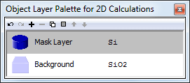
A variety of sensors and excitors can be added. In this case we used a mode excitor which calculated and injected the fundamental TE mode in the form of a sinusoidal pulse in the time domain. Sensors were added at the input, the through port and the drop in just a few clicks. For 2D calculations, each colour on the layout is associated with a given material. In this case we used a pre-defined silica model from the material database provided with OmniSim.
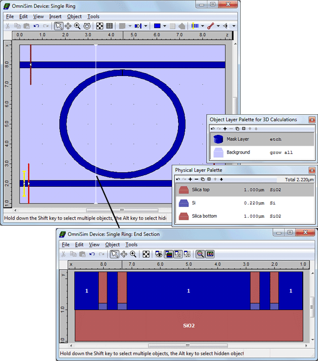
Design of a ring resonator in 3D using the OmniSim Layout EditorDesigning photonic devices in 3D using OmniSim is extremely easy: start by defining an epitaxial structure along the vertical direction and you can then define masks for the "etch", "fill" and "grow" operations that you would use to create your physical structure. In this case we will grow an epitaxial structure composed of silicon embedded in silica and we will then etch it to create the ridges for the rings and the bus waveguides. The mask layer will be defined using the shapes used to design the 2D structure: you can easily design the 2D and 3D device at the same time!
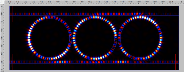
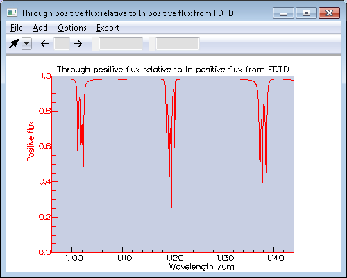
FDTD calculation of the resonator spectrumThe FDTD calculations were performed on 16 SMP (symmetric multi-processing) threads of an Intel Xeon CPU E5620 working at 2.4GHz. A uniform grid spacing of 50nm was used for the 2D calculation of the three coupled SOI rings. The duration of the 2D calculation was set to 300ps (~2.1e6 time steps). You can run the video below for a live recording of the 2D FDTD calculation: The resonances were characterised by plotting the spectrum of the flux in the Through sensor relative to the flux in the Input sensor. The results can be seen below, clearly showing the degenerate peaks due to the coupling between the rings.
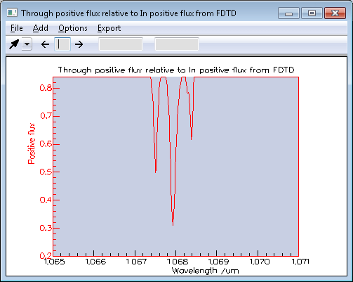
A uniform grid spacing of 50nm was used for the 3D calculation of the single SOI ring. The duration of the 3D calculation was set to 12.5ps (~131000 time steps). The resonances were characterised by plotting the spectrum of the flux in the Through sensor relative to the flux in the Input sensor. The results can be seen below.
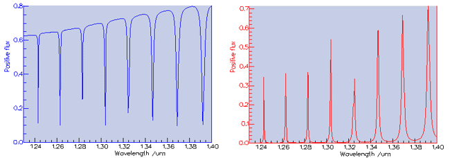
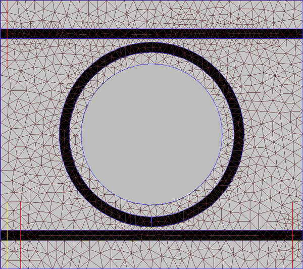
FETD calculation: using void regionsIt is also possible to simulate this structure in 2D and 3D with our FETD Engine. Although FDTD will be able to generate results with reasonable accuracy in a small amount of time, you can switch to FETD when you need high precision as FETD offers faster convergence than FDTD. Being able to switch between FDTD and FETD offers you a very efficient way to perform convergence tests. Another benefit of FETD is that it allows you to exclude parts of the structure from the simulation by defining void regions, in order to speed up the simulations. You can see this applied below to our ring resonator; we have specified a void region in the centre of the ring, where the fields will not be computed. This feature is particularly useful for large ring and disk resonators.
|
 © 2023 Photon Design copyright all rights reserved |

 |