|
Introduction
Features
‣
Model Details
‣
Interface
‣
Simulations
‣
XY Laser Module
‣
VCSEL Module
‣
Harold QCSE
‣
Link
to PICWave
‣
Scripting / Optimisation
Applications
Options
Publications
Download Brochure
Request evaluation
|
Simulations
Harold Simulations
A HAROLD device simulation consists of solving the governing equations of the model at a set of bias currents, so as to obtain the characteristics of the device vs. current.
HAROLD has a number of simulation modes to choose from:
-
Running mode
-
1D: Solves self-consistently the various differential equations of the model in the vertical (y) direction only, assuming uniformity on the longitudinal (z) direction.
-
2D (XY, option): as above but models variations
of electrical and optical fields in both transverse directions.
-
2D (YZ): Solves self-consistently same equations as in 1D mode but also considers longitudinal effects such as surface recombination and optical absorption at facets, and the non-uniformity of the optical field.
-
PICWave Model: a variation of the 1D isothermal model, this mode is used for producing material gain models which can be exported to PICWave.
-
Execution mode
-
Isothermal: Simulates the device under “pulsed” operation i.e. ignores heating such that the temperature is fixed at a constant value throughout the whole structure.
-
Self-heating: Simulates the device under “CW” operation i.e. accounts for device heating model the heatflow within the device
-
Test: A quick diagnostic mode which simulates the device at zero bias - it allows you examine basic results so you check that your layer structure has been set up as intended.
Simulation Results
Due to its detailed physical model, HAROLD can obtain a wide range of simulation results, including:
-
1D/2D Results (i.e.
vertical/vertical-longitudinal profiles):
-
Electrostatic potential, electric field
-
Electron and hole Fermi energies
-
Conduction and valence band edges
-
Electron and hole densities (in bulk and QWs)
-
Electron and hole current densities
-
Recombination rates: SRH, Auger, spontaneous
emission, stimulated
-
Heat flow and temperature profiles, profiles of
different heat sources (Joule effect, non-radiative recombination, free-carrier absorption)
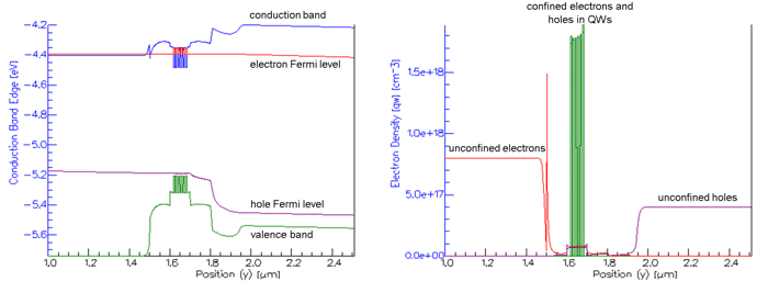
(left) Alignment of electron and hole Fermi energies with conduction and valence bands in
InGaAsP 1.55µm 6QW epi-structure and (right) profile of confined and unconfined electron and
hole densities in same structure – vertical leakage of unconfined carriers through QWs can be seen
-
Per-bias Results (i.e. vs. bias current/voltage/current density):
-
Optical powers for left and right-hand facets (optical output power, scattered and absorbed power)
-
Dissipated power due to Joule heating, non-radiative
recombination, free carrier absorption
-
External slope efficiency for both facets (dP/dI)
-
Electron and hole densities (in bulk and QWs)
-
Active region temperature
-
Quantum efficiency
-
Lasing wavelength
-
Modal and material gain
-
Effective mode index change
-
Free carrier loss
-
Recombination rates (in bulk and QWs): SRH, Auger, spontaneous emission, stimulated
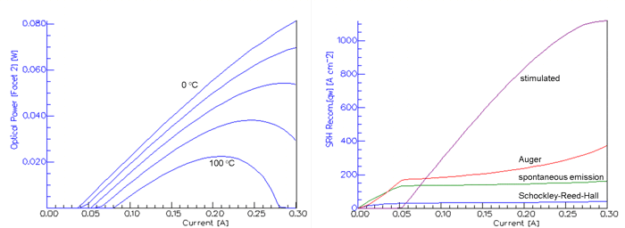
(left) LI curves for self-heating laser diode simulation for ambient temperatures 0C to 100C
and (right) recombination rates for 50C ambient temperature simulation –
the rising Auger contributes to the thermal roll-over in the LI curve
-
Spectra:
-
Gain
-
Spontaneous emission
-
Refractive index
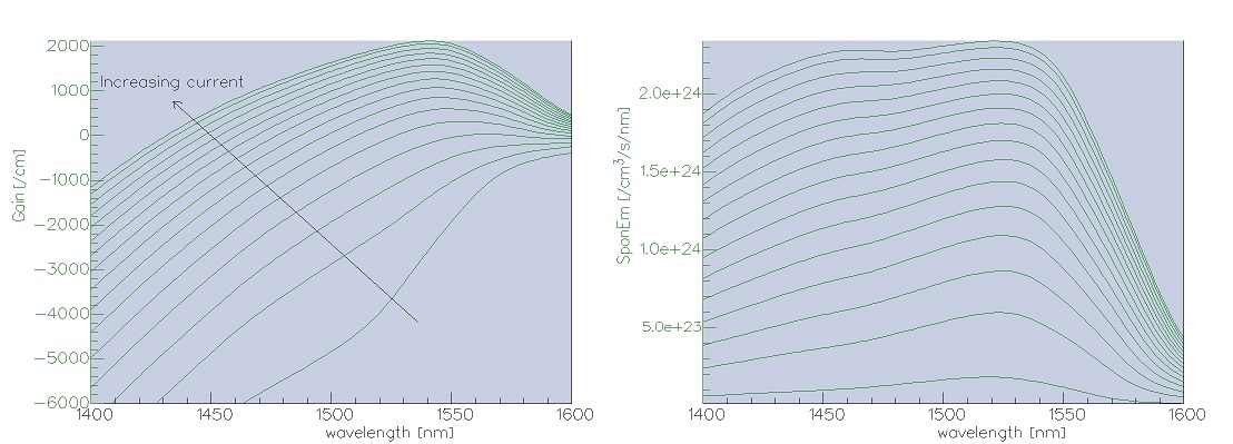
Gain (left) and spontaneous emission (right) spectra for the set of simulated biases (isothermal simulation)
-
Quantum well results:
-
Electron, light-hole, heavy-hole potentials
-
QQW wavefunctions and energy eigenvalues for electron, light-hole and heavy-hole sub-bands
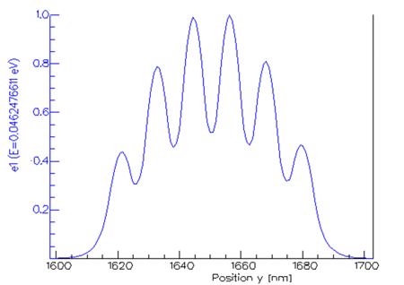
Wavefunction of the lowest energy electron state in a 6 QW structure
|