|
|
Your source of photonics CAD tools | |
|
| ||
FIMMWAVEA powerful waveguide mode solver |
    |
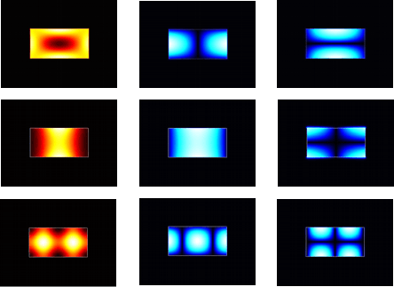
The FDM SolverA finite difference mode solverFIMMWAVE includes an advanced finite difference mode solver: the FDM Solver. It is implemented in a fully vectorial way. It supports non-uniform meshes, with automatic refinement in regions where higher resolution is needed. Advanced techniques make Photon Design's implementation of the finite difference method substantially more accurate than has been available up until now from this method.
The FDM Solver is very fast on absorbing devices or metallic waveguides for which a complex solver is needed. PML layers are implemented, allowing one to model radiation or leakage. The FDM Solver is also particularly well suited to model waveguides with high-step refractive index profiles, slanting/curved interfaces and gradient profiles. It is therefore a very good choice for applications in silicon photonics. It can also be used in its complex version to calculate bend modes. FeaturesFully-vectorial and semi-vectorial versions
The FDM Solver supports perfect electric wall and perfect magnetic wall boundary conditions, Impedance boundary conditions (anywhere between the perfect electric wall and the perfect magnetic wall), Transparent boundary conditions, periodic boundary conditions and Perfectly Matching Layers (PMLs). Structures for which the FDM Solver is recommended:High index contrast waveguides.
See also the Mode Solver Features Table for comparison with other solvers.
|
 © 2023 Photon Design copyright all rights reserved |

 |