|
|
Your source of photonics CAD tools | |
|
| ||
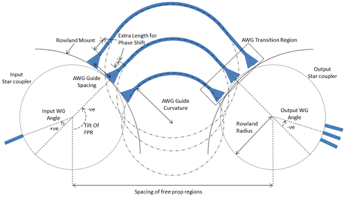
EPIPPROPA WDM/DWDM model for AWGs and Echelle Gratings |
   |
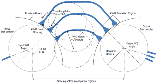
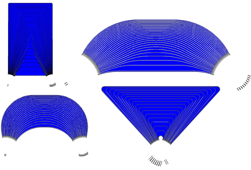
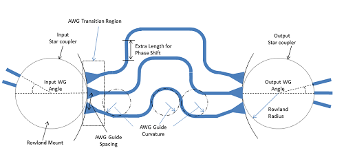
Design Templates for Arrayed Waveguide GratingsThe AWG model leverages Photon Design’s experience in both waveguide modelling and free propagation region expansion to create an ultrafast simulation and design tool for the creation of bespoke wavelength division multiplexing devices. The Epipprop AWG option includes four AWG template designs that can be rapidly used to create designs:
These two template designs build in lots of flexibility in shape and layout. Compact designs can be rapidly prototyped, modelled and exported to GDSII for manufacture. The designs come with a built-in linear adiabatic taper model for the transition region along the edge of the star coupler. More complex tapers (parabolic, horn, etc.) and neighbour coupling can be modelled using the connection to our sister product FIMMPROP. One can also use FIMMPROP to model channel broadening using Multimode Interferometer input/output waveguides. Fixed Bend Radius AWG Design
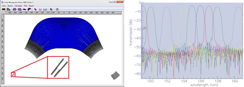
You can see below an example of Fixed Bend Radius AWG design in which we have used MMIs and FIMMPROP to model the broadened response of an AWG designed in a Si3N4 platform.
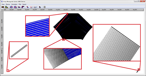
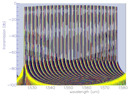
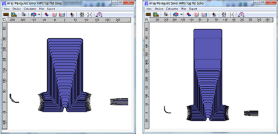
Epipprop is platform agnostic and can be used to model low-index contrast AWGs (silica) as well as high-index contrast AWGs (SOI) or anything in between (e.g. silicon nitride)! The design tool can include any user-defined material and take into account any material dispersion in the design layout. You can specify the spacing between the waveguides at the output waveguide array in terms of wavelength or frequency spacing, allowing you to concentrate on the geometry of the arrayed waveguides and not worry about continuously adjusting the output waveguide positions as Epipprop does it automatically. You can see below the design of a 256 channel AWG designed in a silica platform. The footprint of the device is 49x86mm2 with waveguides tapering from 15um to 4.5um, showing Epipprop's versatility in modelling a device with features over 3 orders of magnitude smaller than its size!
A great variety of AWGs can be created using just this one template as shown here!
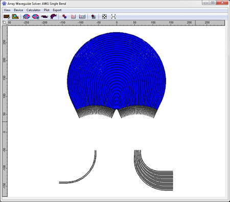
Single Bend Per Path Template
Each waveguide in the array follows a path with a single bend between the star couplers. To allow the physical layout of an AWG then each path must have a different radius of curvature. EPIPPROP will rigorously model all the modes in the straight and different radius bend sections and take into account the different propagation constants to ensure that the user requested phase difference is maintained across the whole array.
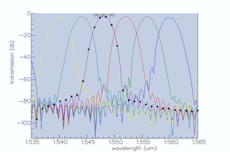
Here we have an example of a layout in Silicon on Insulator. The design has all input and output waveguides uniformly spaced and aligned horizontally to allow easy integration into larger designs. The total size is 320x440um and splits the light into 6 channels spaced by 4nm. Shown below is the results modelled in EPIPPROP taking into account the modes in each deep etch waveguide and effective indices of the modes in all the varying bends.
“Top Hat” AWG Design Template
Each waveguide is aligned to the horizontal after the AWG transition region, and then follows a path entailing four 90° bends, allowing for a compact design. EPIPPROP allows you to adjust the path lengths in the layout to simulate slight errors in manufacturing, or calculate the path lengths such that they are all tuned to the central operating wavelength of the AWG.
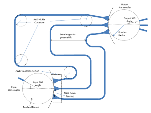
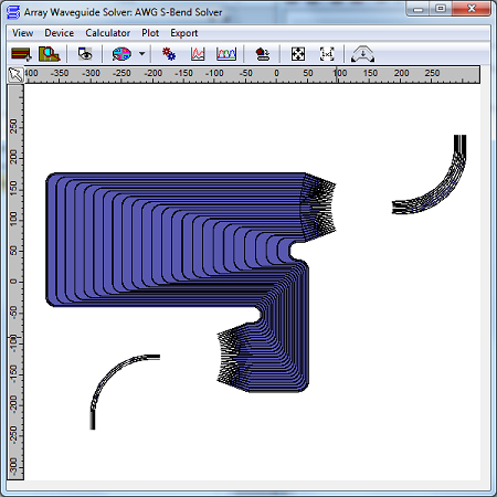
S-Bend AWG Design Template
Similar to the “Top Hat”, the S-Bend allows a compact layout and adds some versatility for integration into larger designs with its vertical offset between star couplers. EPIPPROP automatically minimises the distance between the star couplers for the smallest footprint the AWG will allow!
|
 © 2023 Photon Design copyright all rights reserved |

 |