|
|
Your source of photonics CAD tools | |
|
| ||
CrystalWaveA powerful photonic crystal simulator |
    |
Photonic Crystal Circuit OptimisationSimulation with Kallistos and CrystalWave FEFD softwareKallistos was used to optimise a photonic crystal Y-junction defined and simulated in CrystalWave with the FEFD Engine, allowing us to obtain lossless power splitting over a wide range of wavelength. The initial Y-junction design had high loss due to reflections at the tip of the splitter and the sharp angle of the bend. We performed two successive optimisations with Kallistos:
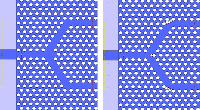
Setting up the optimiserThe structure is shown below before and after the introduction of the atoms.
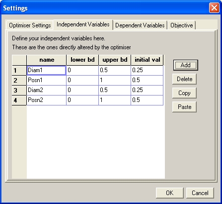
Both optimisation processes were very similar and were performed independently. We will describe here the introduction of the atoms at the tip of the junction. We defined four independent variables: Diam1 and Diam2, which defined the diameter of the two atoms, and Posn1 and Posn2 which defined the position of each of the atoms along the horizontal axis. For each of these variables, we selected a suitable range of variation.
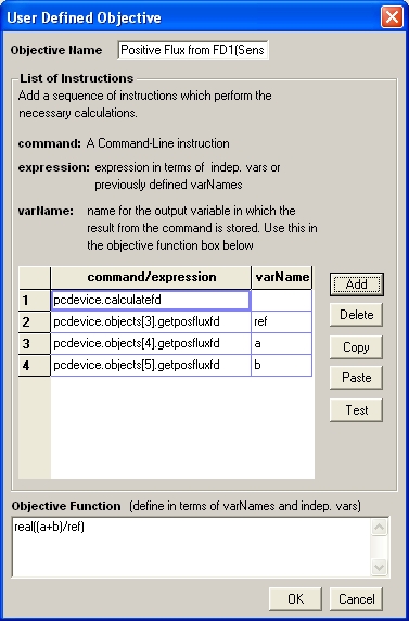
We then chose a simulation engine. In this case we decided to simulate the structure at each optimisation setp using CrystalWave's FEFD Engine, a very fast and powerful 2D propagation tool, which is ideal for fast optimisation. We defined an objective function for Kallistos to optimise. Although Kallistos can choose from a range of pre-defined objective functions, it is also possible to choose an arbitrary function based on the extensive command line interface, which is what we did here. This allowed us to ask Kallistos to maximise the sum of the flux through the two output branches divided by the flux through the input sensor, i.e. to maximise the total transmission. The user-defined objective function is shown below. Learning the commands is very easy: they are displayed in a command line window when performing simulations using the user interface!
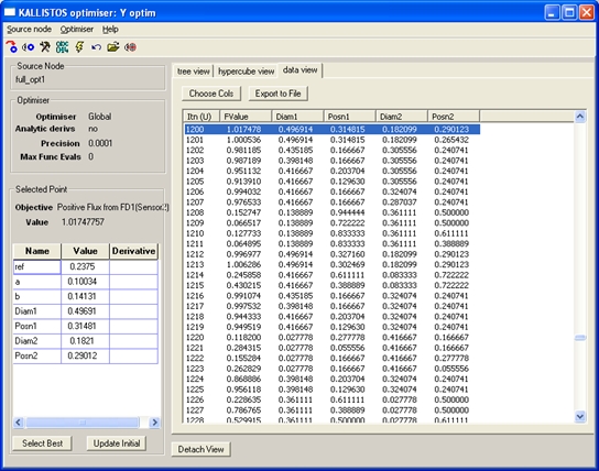
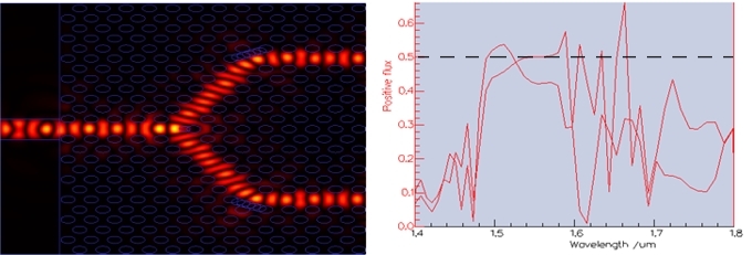
Optimisation results: from quasi-total loss to ~96% transmission!We run the optimisation using Kallistos' Global optimisation algorithm. This allowed us to find range of different solutions in different parts of the parameter space, which were then inspected to find the most suitable solution for fabrication purposes.
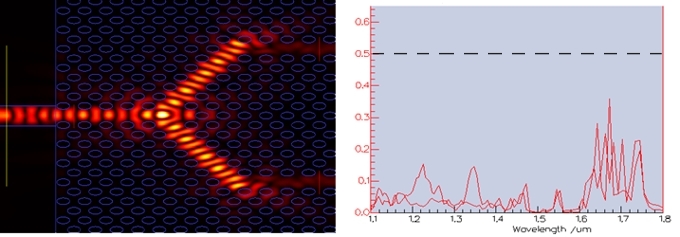
The optimum design is shown below. You can see below the transmission in the structure before the optimisation at the top, and the optimised structure at the bottom. In each case, the result of the FEFD simulation is shown on the left-hand side and the transmission spectrum into each branch is shown on the right-hand side. Although the transmission in each branch did not exceed 30% before optimisation, a transmission of above 90% (sum of the two branches) was obtained over the pass band of the line defect (from 1.5um to 1.6um) after the optimisation.
|
 © 2023 Photon Design copyright all rights reserved |

 |