|
|
Your source of photonics CAD tools | |
|
| ||
PICWaveA photonic IC, laser diode and SOA simulator |
    |
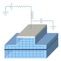
Electrical modelPICWave has extensive capabilities for accurately modelling the electrical aspects of your active photonic components, including diode IV characteristics, current spreading, travelling wave (microstrip) effects and external electrical circuits composed of resistors, inductors and capacitors.
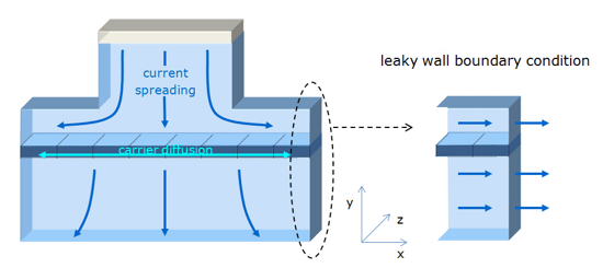
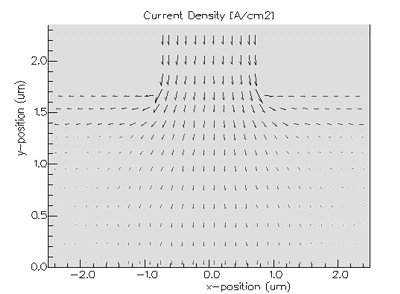
Current spreading and leakagePICWave can model the current spreading within the cladding regions of gain sections based on mobility and doping, as illustrated below. The current spreading model supports near-arbitrary, rectangle-based cross-section geometry, and also allows multiple electrical contacts and insulating regions. Furthermore, it can also model the leakage of current through the left and right boundaries of the simulated region of the cross-section using an appropriate boundary condition.
PICWave can thus be used both to assess the impact of lateral current spreading/leakage on the performance of lasers, and also to simulate SOI hybrid lasers with n and p-contacts on the same side, where lateral current flow is crucial to laser operation.
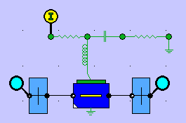
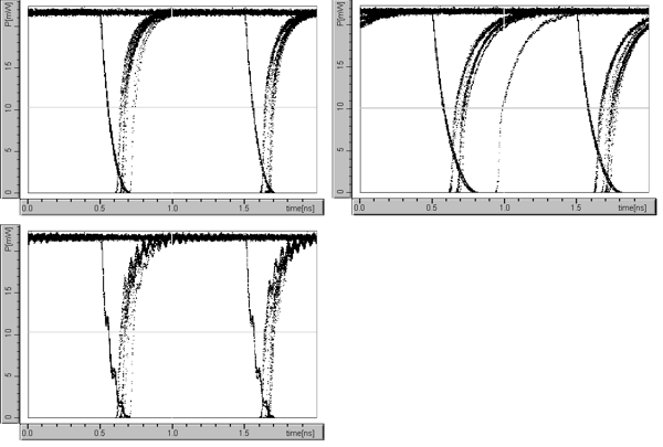
Electrical componentsNear-arbitrary electrical circuits can be constructed from inductors, capacitors, resistors, electrical nodes and electrical drives. These can be attached to active sections and the electrical-optical interaction modelled e.g. the effect of parasitics on laser operation, or the electrical response of a photo-detector etc. The example below shows an FP laser modulated by a current data signal via a drive circuit containing an inductor and capacitor.
The effect of the capacitance and inductance on the laser output is shown in the oscilloscope plots beneath.
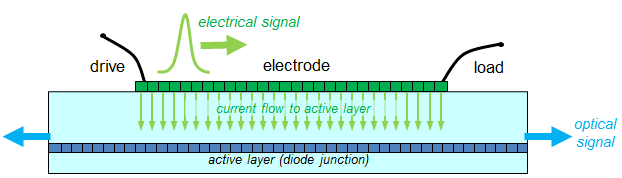
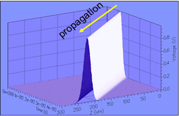
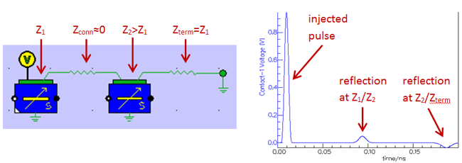
Travelling Wave ElectrodeElectrodes on active sections can be modelled as travelling wave electrodes with a defined inductance and capacitance per unit length. These electrodes can in turn be connected together or connected to other elements using the LCR connections described above. This enables one to model the propagation of electrical signals along the electrode and any reflections that occur due to impedance mismatches at connections or terminations. A key application of this feature is modelling travelling wave modulators.
This advanced algorithm will even alter the microwave impedance as a function of bias voltage, i.e. taking into account the variation of diode impedance with diode bias voltage.
|
 © 2023 Photon Design copyright all rights reserved |

 |